For our electronic devices, such as phones, to shrink, the electronic components used inside them also need to shrink and this has led to “chip-scale packaging” where the chip package is not much larger than the bare silicon die inside it - but how does this affect security?
Chip packaging
To start to look at the issue, we need to have some understanding of how chips are manufactured and produced into a form that we can then add to our device’s printed circuit board.
The core of every chip is a microscopic electronic circuit that is built from layers of semiconductor materials and metals on top of a semiconductor substrate (usually Silicon, although this could also be a more exotic material such as Gallium Arsenide). This circuit, called a “die”, is typically a few mm in size and its connections to the outside world are made through a number of small metal “bond pads” which are normally distributed along the edges of the die, forming a “pad ring”.
The pad ring is much too small to solder directly on to and the die itself is relatively fragile and can oxidise in air, so the die pads need to be brought out to the larger external connections (such as pins, leads or balls depending on the technology) and the whole lot put in a package to make it more robust and useful.
Traditional packaging technologies from the earliest through-hole DIP packages to more recent surface-mount QFP and QFN packages connect tiny wires called “bond wires” from the pad ring to each external pin, lead or pad on the packaged device and encapsulate the whole device in a robust material. A cross section of a QFP device is shown below.

The “front side” of the die with the pad ring faces upwards in this type of packaging.
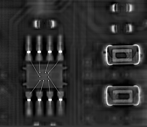
You can see the chip leads, bond wires, pad ring and other internal parts of the chip in the high-resolution X-Ray CT scan image horizontal slice of a circuit board below that we made during a reverse engineering job. The other components visible are surface mount chip capacitors and you can also see some effects from the PCB tracks and vias lower down.

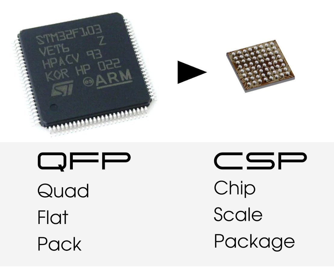
The push for smaller die packaging has led to “Chip Scale Packaging” (CSP), which according to J-STD-012 must have a package area less than 1.2 times that of a single die. There are a number of practical reasons as well as just size for CSP devices, including a better electrical connection to the die resulting in better signal integrity, and easier packaging amongst others.
There are a number of variants of CSPs, but we’ll look at one of these called the Fan-In Wafer-Level Package (FI-WLP) Wafer-Level Chip Scale Packages (WL-CSP) variant, which is a “true” CSP according to the definition given previously. A cross-section of this WL-CSP is shown below.

As you can see from the diagram, the significant differences are that bond wires are replaced by a “redistribution layer” that wires the pad ring (facing down this time) onto a regular set of bumps through copper tracks and posts (a replacement for the leads/pins). These can then be soldered to the circuit board directly. The amount of chip packaging material used is considerably less, with only a very thin layer coating the top and edges to give a small amount of protection to the die and allow a surface for marking the component details on.
For more information on CSP and some nice microscope pictures of real chips, see this article at EDN.
So what’s the problem?
In 2015, a Raspberry Pi 2 owner was photographing his new board and found that every time the flash on his camera went off, the Pi powered down. This effect, called the Xenon Death Flash was traced to the processor core voltage regulator chip - in a WL-CSP package. Many manufacturers producing WL-CSP devices assume that they will be safely contained within a dark enclosure, but what if we are deliberately trying to attack them?
There are a number of ways that a chip can be physically attacked from the backside including:
- Infrared (IR) lasers can be used through the substrate or the edges of the die (lateral laser fault injection (LLFI)) to inject transient faults
- A Focused Ion Beam (FIB) can dig cavities in the substrate to allow probing of metal lines underneath
- Electromagnetic (EM) emissions can be recorded at different points over the die to look for information leakage
- EM pulses can be used to inject transient faults
- A probe can apply a voltage to the backside, known as Body Biasing Injection (BBI), to induce a transient fault
- Photon emission analysis is possible, where the opposite of the Xenon Death Flash occurs and the working device causes photon emission during its operation, potentially leaking information
With the exception of the EM attacks, these require that the bare die can be accessed and are called “invasive attacks”. For traditional chip packaging, “decapsulating” or “decapping” the package to expose the die can be difficult to do and requires time, patience and usually dangerous chemicals such as Nitric acid. For an example of someone trying (sucessfully!) this process for the first time, see this website - it also has some very nice photos of decapsulated chips showing the die and bond wiring.
As there is considerably less packaging material on a WL-CSP (and it is usually a polymer coating that can be scraped off with a sharp knife), this process becomes a lot easier - and may not even be necessary as can be seen from the Xenon Death Flash example.
For the EM attacks, if we can get closer to the die with the EM probe, then we’ll get a better localised signal or region to cause a fault in. For example, we may be able to more reliably fault a specific part of a cryptographic processor that could then result in information leakage. For an example of a commercial tool for this (as well as a nice photo of this attack being applied to a QFP chip), see this webpage for Langer’s ICI HH500-15 L-EFT Pulse Magnetic Field Source.
In 2020, Colin O’Flynn (creator of the excellent low-cost side-channel attack platform ChipWhisperer and EM fault injection tool ChipSHOUTER) released a paper titled “Low-Cost Body Biasing Injection (BBI) Attacks on WLCSP Devices” in which he developed a $15 tool, which was then used to attack the hardware blocks within an STM32F415OG microcontroller.
The front side of the die may also be a target, as much of the die can still be exposed. This requires micro-wiring to the bumps to make the device functional and even the removal of some bumps to expose more die area.
With the increasing use of this type of packaging, even for secure chips, there will almost certainly be an increased interest from attackers.
What can be done?
Avoiding such attacks is not easy and depends on the chip, security level required, and other physical factors. One option may be to cover WLCSP devices with epoxy making it harder to reach the die, although this can have negative effects on things like heat dissipation. More physically secure enclosures may be another option.
There are also some proposals for chip packaging countermeasures that protect against backside attacks, such as the one presented in the paper “A Novel Structure for Backside Protection Against Physical Attacks on Secure Chips or SiP” or for die-level countermeasures such as those demonstrated in the paper “Nanopyramid: An Optical Scrambler Against Backside Probing Attacks”. Both of these require implementation at the die production and packaging stage.
In the end, you will need to determine the risk of using such devices and ensure that the ones you select have security countermeasures implemented by you or the manufacturer that can withstand the potential attacks that your device may experience.
How can we help?
If you need help to secure your hardware (or software), then please contact us through the web contact form or email.
